 | |||||
The microstrip patch antenna takes on many forms and has been widely used in the past due to its low profile and ease of manufacturing. There are many different types of microstrip patch antennas, and many of them can be found in the MicrowaveTools Antenna A-Z database. While this type of antenna is not used as much as it once was, the theory behind this antenna has led to many of the more modern antennas such as the IFA, PIFA, and FICA antennas. All the equations for determining the size and impedance of an inset fed patch antenna are at the end of this post. Matlab scripts are provided.
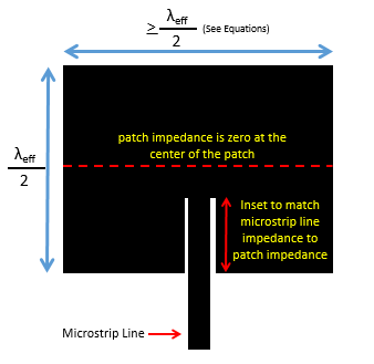
Dimensions of a traditional inset fed patch antenna
A well designed patch antenna can have a peak gain between 6 and 8dBi, and as such it is considered to have a directional pattern (click to rotate 3D image below) which is linearly polarized along the width of the patch.
Rotate Image by clicking on the image and moving the mouse
The rectangular patch is one of the more common types of patch antennas. This antenna is designed using a rectangular piece of electric conductor situated above a ground plane. The rectangular piece of copper measures 


The natural input impedance of a patch antenna dependent on where within the patch the feed is located. It is possible to match the patch antenna from below 30Ω to above 200Ω. If the feed is located closer to the edge of the patch the input impedance will be high, if the feed is located closer to the center of the patch the impedance will be low. Below is the standard input impedance of an inset fed patch antenna at 2.45GHz.
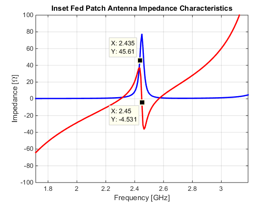
Typical impedance of a inset fed patch antenna
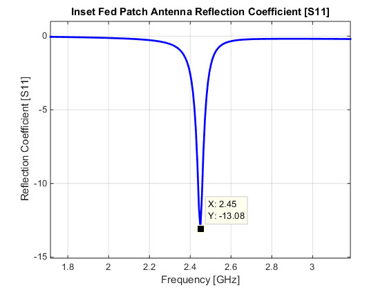
The 50Ω bandwidth of a patch antenna designed to have a resonance of 2.45GHz is shown below. This type of antenna is inherently a high Q antenna, meaning that this antenna is relatively narrow banded.
Typical impedance of a inset fed patch antenna
There are many different ways to feed a patch antenna, the inset fed patch antenna is fed via a microstrip feed line connected to a specific point within the patch. Through varying the location of where the microstrip connects to the patch antenna the measured input impedance can be controlled. In the reflection coefficient shown above was matched to a 50Ω microstrip line.
The Microstrip patch antenna is a little different than many antennas, as the structure itself does not radiate, but rather the edge gaps between the patch and the ground plane. This can be visualized below. line is situated directly above where the patch radiates from, this effects the pattern of the patch antenna and what applications it can be used in. The areas where the patch radiates from are shown below.
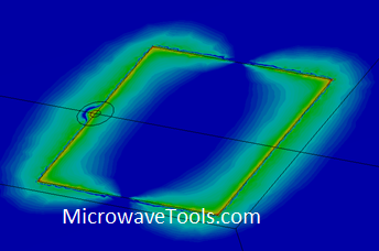
The patch antenna radiates from the side in which it is fed and the opposite side.
The patch radiation is effected by the microstrip line, due to the microstrip line “blocking” some of the radiation. This creates a skew in the pattern, causing the boresight of the antenna not being located exactly normal to the planar surface of the patch antenna. A typical skew is between 3º and 8º depending on the width of the microstrip feed. This means that it is not possible to make an inset patch radiate with circular polarization without using four feeds.
General Facts:
- Larger Patch = Lower Frequency
- Thicker Dielectric = More Bandwidth
- Center of patch = 0Ω
- Edge of patch >200Ω
- Pattern skewed by microstrip inset
- Patch radiates from two “slots” in ground plane
Design Guidelines:
- Patch Width
- Patch Length
- To Increase Frequency:
- Decrease Patch Length
- Decrease dielectric constant
- Increase Bandwidth:
- Increase patch distance from ground
- To a lesser extent:
- Increase patch width
- Decrease dielectric constant
- Increase input impedance by reducing the feed inset
- Inset Spacing
microstrip width


More in depth understanding of the inset Patch Antenna
(Matlab/Fremat Links at End):
The inset patch design has three distinct geometrical regions. The first is the actual patch itself. The second is the feed line. Finally, the third part is the ground plane. It is possible to derive the parameters of patch antenna using a few different techniques. This article will focus on the cavity model approximation in most situations and will fall back on the transmission line model to derive parameters such as the input impedance of the patch.
It is possible to determine the width of the patch, w, using Equation (1). The width of a patch antenna is good starting point when designing a microstrip patch antenna. This is due to the width not having a significant impact on the operational frequency of the antenna, and tends to have the largest effect on the bandwidth and the input impedance (excluding dielectric height and constant) of the patch antenna.

Equation 1
Prior to determining the length of the patch, L, the effective permittivity of the substrate, εreff, must be calculated from Equation (2).
![\epsilon_{reff}=\frac{\epsilon_r+1}{2}+\left[\frac{\epsilon_r-1}{2} \left (1+12\left ( \frac{h}{w} \right )^{-1/2} \right ) \right ] \approx \epsilon_r](http://s0.wp.com/latex.php?latex=%5Cepsilon_%7Breff%7D%3D%5Cfrac%7B%5Cepsilon_r%2B1%7D%7B2%7D%2B%5Cleft%5B%5Cfrac%7B%5Cepsilon_r-1%7D%7B2%7D+%5Cleft+%281%2B12%5Cleft+%28+%5Cfrac%7Bh%7D%7Bw%7D+%5Cright+%29%5E%7B-1%2F2%7D+%5Cright+%29+%5Cright+%5D+%5Capprox+%5Cepsilon_r&bg=ffffff&fg=000000&s=2 "\epsilon_{reff}=\frac{\epsilon_r+1}{2}+\left[\frac{\epsilon_r-1}{2} \left (1+12\left ( \frac{h}{w} \right )^{-1/2} \right ) \right ] \approx \epsilon_r")
Equation 2
The length of the patch is determined by the electrical length of the antenna rather than the physical length of the antenna. The effective dielectric constant impacts the speed at which electric energy travels through this media. This effectively changes the resonant frequency of the antenna. To design the length to match the required resonant frequency Equations (3), (4), (5) are used.

Equation 3
(\frac{w}{h}+0.264)}{(\epsilon - 0.258)(\frac{w}{h}+0.8)}")
Equation 4

Equation 5
The actual length of the antenna is determined by two factors: the effective length, Leff, and the correction factor, ΔL. The effective length is a calculation of the electrical short based on the design wavelength and substrate. The correction factor is a heavily refined formula to account for the exact dimensions of the substrate. [4]
After calculating the patch length, the feed line characteristics can be determined. There are many different feeding types that can be implemented in a patch antenna; in this particular patch antenna an inset microstrip feed will be used.
In order to determine the approximate input impedance of the patch antenna, many different approaches have been derived. One in particular is derived in [1] by analyzing the patch antenna as two slot radiators. In this derivation the admittance is calculated using Equations (6), (7), and (8).
+k_0Ws_i(k_0W)+\frac{sin(k_0W)}{k_0W}}{120\pi^2}")
Equation 6: where  is the Sine integral function
![G_{12} = \frac{1}{120\pi^2} \int_{0}^{\pi} \left [ \frac{sin ( k_0 W cos(\theta)) }{cos(\theta)} \right ] J_0 (k_0L\ sin(\theta))\ sin^3(\theta) \ d\theta](http://s0.wp.com/latex.php?latex=+G_%7B12%7D+%3D+%5Cfrac%7B1%7D%7B120%5Cpi%5E2%7D+%5Cint_%7B0%7D%5E%7B%5Cpi%7D+%5Cleft+%5B+%5Cfrac%7Bsin+%28+k_0+W+cos%28%5Ctheta%29%29+%7D%7Bcos%28%5Ctheta%29%7D+%5Cright+%5D+J_0+%28k_0L%5C+sin%28%5Ctheta%29%29%5C+sin%5E3%28%5Ctheta%29+%5C+d%5Ctheta+&bg=ffffff&fg=000000&s=2 "G_{12} = \frac{1}{120\pi^2} \int_{0}^{\pi} \left [ \frac{sin ( k_0 W cos(\theta)) }{cos(\theta)} \right ] J_0 (k_0L\ sin(\theta))\ sin^3(\theta) \ d\theta")
Equation 7
}")
Equation 8
The above derivation of the patch input impedance is a good starting point. However, due to the derivation not accounting for material properties, such as material losses, this derivation only sets an upper limit on the input impedance.
Once the edge impedance is derived, the next design parameter is to properly interface the feed line impedance with the patch antenna impedance. The current to voltage ratio changes as a function of 
 = R_{edge}\ cos^2 \left ( \frac{\pi y_0}{L} \right )")
Equation 9
 = R_{edge}\ sin^2 \left ( \frac{\pi y_0}{L} \right )")
Equation 10
The final design consideration of the patch antenna is to ensure a large enough ground plane is used for this particular derivation. Equations (11) and (12) determine the minimum ground length and width that should be used with this particular design.

Equation 11

Equation 11
The patch cutout for the feed inset should be > 2 times the microstrip width. This means that on each side of the feed line there should be a distance of 1/2 the microstrip width on each side of the microstrip between the microstrip feed line and the patch antenna.
Matlab/Freemat file 1
Matlab/Freemat file 2
Links to Matlab and Freemat websites